Introduction
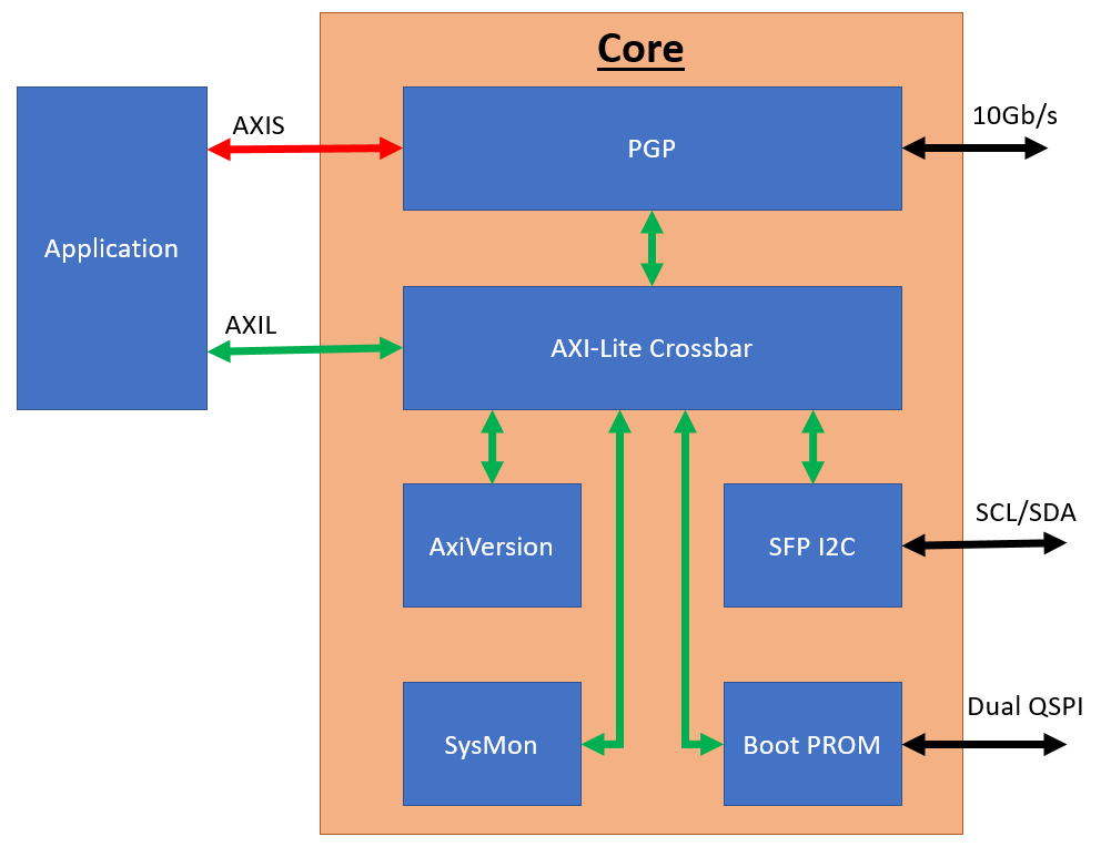
The firmware structure for the present example is divided into two main blocks, Application and Core.
The interfaces between the Core and the Application are AXI-Lite and AXI stream buses.
The AXI-Lite bus is used for register access.
(refer to https://developer.arm.com/documentation/ihi0022/e/)
The AXI stream bus to transfer ASYNC messages to/from the PGP module
(refer to https://developer.arm.com/documentation/ihi0051/a/Introduction/About-the-AXI4-Stream-protocol)
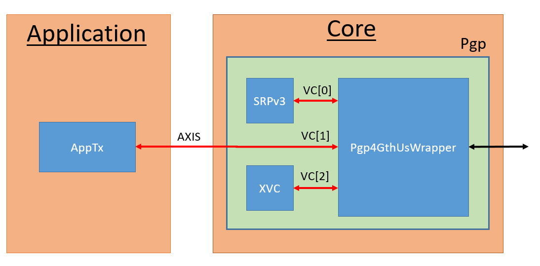
Inside the application block includes a AppTx module. This module is an example of how to produce data on the AXI stream bus. This AXI steam bus is connected to the Core and routed to the PGP module. (refer to https://confluence.slac.stanford.edu/x/1dzgEQ for more information about PGPv4).
A block diagram on this stream path from the Application’s AppTx module to the PGP is shown below:
The Application module is designed to be a “template” for developers. They can copy the firmware modules and structure then customize it to their specific applications. Developers can treat the core module has a Board Support Package (BSP).

